CHAPTER 2 LITERATURE REVIEW
This section will analyze some research that has already been done and give a short description of different mechanisms and the significant theories to this report.
2.1 The control of PWM
The control of PWM is a method where DC static input voltage is fed to the inverter and the result is a meticulous voltage in AC. This is prepared through regulating the OFF and ON inverter periods components. Its advantage is that harmonics of lower orders are minimized or removed with the voltage control outputs. Therefore, the filtering necessities are reducing because the higher orders’ harmonics can easily get filtered (Mounika, 2013).
In the sinusoidal modulation, more pulse for every cycle are employed and the pulse width is a sine wave function for angular pulse cycle position in a cycle. Triangular of a higher frequency wave voltage is comparable to the pulse which has been modulated. The switching moments and commutation of the modulated pulse are decided by the crossing point of Vc and Vr waves. The reference and carrier waves are mixed in a comparator ( Profumo, 2012) . The 3 Phase Inverters employ Pulse width modulated signals to control the three-phase motors. The principle of operation is that the control algorithm can be encoded in the pulse width generated for inverter operation. The two components of the PWM signals are the frequency and the signals’ duty cycle.
The duty cycle defines the amount of time for which the pulse will be high, and the frequency defines the number of produced cycles for every second (Urmila, 2010). By varying the widths of the pulses generated, the OFF and ON time of the switches in the main inverter topology is controlled, giving an output of the desired voltage. When filtered by the high inductance of the motor, this voltage provides sinusoidal current to the motor windings. Three sets of one high side and one low side switch signals each are generated corresponding to the three arms of the inverter connected to the three phases of the motor ( Muttalib, 2012). The signals are encoded in such a way that none of the high side switches gets connected to the low side switch in the same arm for even the shortest time window for the obvious reason of avoiding short circuit between the positive and negative DC rail.
PWM principle
The below diagrams illustrate the principles of PWM.
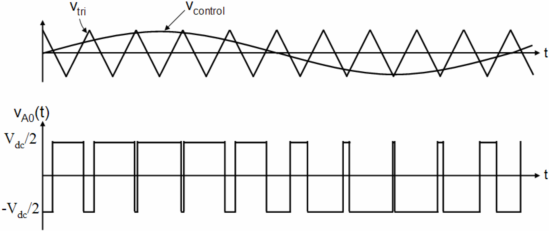
As illustrated in the above figure, the output voltage of the inverter is obtained as following:
The following properties characterize the inverters’ output voltage;
The frequency Vtr is equals to the pulse modulated frequency
The inverters amplitude can be adjusted by the value of peak voltages
The fundamental frequency is controlled through the voltage control frequency.
The index of modulation (m) can be defined as below
Where, (VA0)1: fundamental frequency component of VA0.
2.2.1 Sinusoidal Pulse Width Modulation
SPWM (Sinusoidal pulse width modulation) gives a sinusoidal waveform through the pulse wavelength’s filtration with varying width. The suitable voltage at the output is obtained through changing the amplitude and the frequency (voltage modulating) (Subsingha, 2016). As in Figure 1 above, a waveform of the frequency sine wave is compared to a triangular waveform of high frequency, known as a carrier waveform.
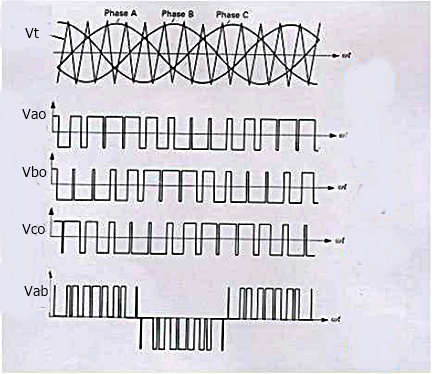
The rate of switching is varied when a sin wave gets intersected with a triangular wave. The position of intersection gives a fluctuating switching time, which is between the states. The waveform of the triangular wave (Vtr) is compared against 3 sine waves control voltage, which is the Vc, Vb and Va and all are at 1200 out of phase to one another (Bellini, 2015). And the level of the waveform is employed to control the device switching in every phase for the inverter as shown in the diagram below;


Space Vector Pulse Width Modulation
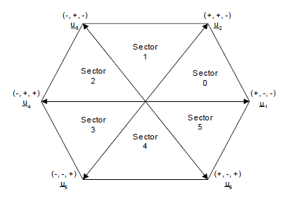
For SVPWM, the duty cycles are computed as opposed to deriving them through comparison as in SPWM. The SVM is based on the illustration of the quantities of 3-phase in a 2-D plane, which is the beta and the alpha. PWM done for the Space vector is very common for 3 phases in inverts. It is usually known as the VSI (voltage source inverters) in fields like in controlling the synchronous permanent and induction motors and AC induction motors. In this project, therefore, I will expand on the modulation of space vector and its implementation since it is very significant in this literature review. The SVM is a common and very sophisticated PWM mechanism used for driving the variable frequency drives, and it is believed that it is the most effective (Ahmed, 2013). Moreover, it is important for the lower total distortion of harmonics. To understand this principle better, the following diagram is used;
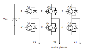
Figure 3: Showing Typical Inverter Topology
It is worth noting that when there is a high side switch that corresponds to a low side switch, it has to be OFF and vice versa to make sure that shoot through current is prevented, which may jeopardize the circuit’s normal operation. And because there are just 3 switches one at a particular time, we will have the bellow 8 switching states;
From the above states, it can be seen that the 1st and the 4th states will produce zero voltage to the motor since they are in order of positive and negatives. Removing these 2 states and then arranging the switches again, we obtain the below sequence of the switching states.
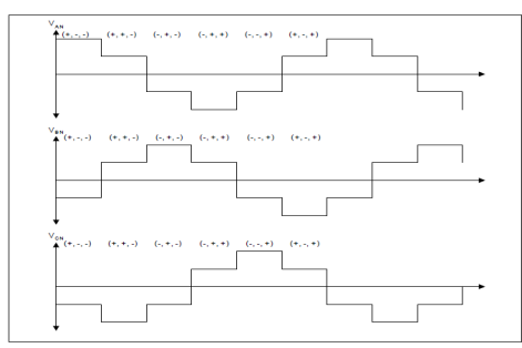
The six states of switching compare to the six steps of voltage, as shown in the diagram above. It is because it can be on the OFF chance that a level of voltage between any 2 voltage steps is actually the 2 comparing varying states are incited in a way that their ordinary outputs are the desired voltage level (Boys, 2010). To form the conditions for the time of any level of voltage, lets change the six voltage steps into six space vectors. When drawn in a 2-D space, the six space vectors outline a hexagon of six divisions. This can be illustrated in the following diagram;
The above figure shows the general 3 phase inverter topology with six switches, three upper and three lowers, with a star connected resistive load. I made this topology using IGBTs on a PCB. The following figure shows the practical implementation.
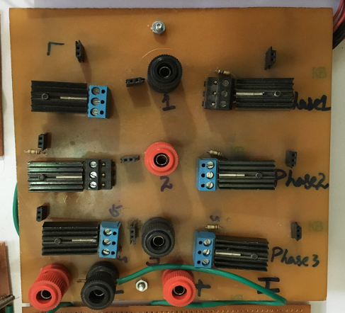
Figure 19. Three half bridge inverter topology using six IGBTs mounted on heatsinks.
The feature of this board is that I used 3-pin connectors. When an IGBT malfunctions due to any reason, I can easily replace it.